Reactive-ion etching
This article needs additional citations for verification. (September 2021) |

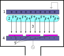
Reactive-ion etching (RIE) is an etching technology used in microfabrication. RIE is a type of dry etching which has different characteristics than wet etching. RIE uses chemically reactive plasma to remove material deposited on wafers. The plasma is generated under low pressure (vacuum) by an electromagnetic field. High-energy ions from the plasma attack the wafer surface and react with it.
Equipment
[edit]A typical (parallel plate) RIE system consists of a cylindrical vacuum chamber, with a wafer platter situated in the bottom portion of the chamber. The wafer platter is electrically isolated from the rest of the chamber. Gas enters through small inlets in the top of the chamber, and exits to the vacuum pump system through the bottom. The types and amount of gas used vary depending upon the etch process; for instance, sulfur hexafluoride is commonly used for etching silicon. Gas pressure is typically maintained in a range between a few millitorr and a few hundred millitorr by adjusting gas flow rates and/or adjusting an exhaust orifice.
Other types of RIE systems exist, including inductively coupled plasma (ICP) RIE. In this type of system, the plasma is generated with a radio frequency (RF) powered magnetic field. Very high plasma densities can be achieved, though etch profiles tend to be more isotropic.
A combination of parallel plate and inductively coupled plasma RIE is possible. In this system, the ICP is employed as a high density source of ions which increases the etch rate, whereas a separate RF bias is applied to the substrate (silicon wafer) to create directional electric fields near the substrate to achieve more anisotropic etch profiles.[1] The RF power given to the substrate is often a tunable parameter called 'platen power', and controls the energy of ions bombarding the surface.[2]
Method of operation
[edit]

Plasma is initiated in the system by applying a strong RF (radio frequency) electromagnetic field to the wafer platter. The field is typically set to a frequency of 13.56 Megahertz, applied at a few hundred watts. The oscillating electric field ionizes the gas molecules by stripping them of electrons, creating a plasma.
In each cycle of the field, the electrons are electrically accelerated up and down in the chamber, sometimes striking both the upper wall of the chamber and the wafer platter. At the same time, the much more massive ions move relatively little in response to the RF electric field. When electrons are absorbed into the chamber walls they are simply fed out to ground and do not alter the electronic state of the system. However, electrons deposited on the wafer platter cause the platter to build up charge due to its DC isolation. This charge build up develops a large negative voltage on the platter, typically around a few hundred volts. The plasma itself develops a slightly positive charge due to the higher concentration of positive ions compared to free electrons.
Because of the large voltage difference, the positive ions tend to drift toward the wafer platter, where they collide with the samples to be etched. The ions react chemically with the materials on the surface of the samples, but can also knock off (sputter) some material by transferring some of their kinetic energy. Due to the mostly vertical delivery of reactive ions, reactive-ion etching can produce very anisotropic etch profiles, which contrast with the typically isotropic profiles of wet chemical etching.
Etch conditions in an RIE system depend strongly on the many process parameters, such as pressure, gas flows, and RF power. A modified version of RIE is deep reactive-ion etching, used to excavate deep features.
See also
[edit]- Deep RIE (Bosch Process)
- Plasma etcher
References
[edit]- ^ Yoo, Jinsu; Yu, Gwonjong; Yi, Junsin (2011-01-01). "Large-area multicrystalline silicon solar cell fabrication using reactive ion etching (RIE)". Solar Energy Materials and Solar Cells. 95 (1): 2–6. doi:10.1016/j.solmat.2010.03.029. ISSN 0927-0248.
- ^ Rawal, D.S.; Agarwal, Vanita R.; Sharma, H.S.; Sehgal, B.K.; Muralidharan, R. (2008-09-30). "A Reproducible High Etch Rate ICP Process for Etching of Via-Hole Grounds in 200μm Thick GaAs MMICs". JSTS:Journal of Semiconductor Technology and Science. 8 (3). The Institute of Electronics Engineers of Korea: 244–250. doi:10.5573/jsts.2008.8.3.244. ISSN 1598-1657.
